A CVSD Audio Digitizer and Playback Device
I designed this circuit in 1985 because I was lonely and needed someone to talk to. The Talking Box would say whatever I told it to say.
Seriously, I had it connected to my phone as a digital answering machine. I had a Data Access Arrangement (DAA) from AT&T that was a telephone line interface and it worked really well. I was playing with touch tones and needed good fidelity. So then the county Family and Children’s Services by mistake put my number on some of their business cards. I got lots and lots of calls, especially because I was writing and reading my salacious trash poetry as my answering message. I am talking hifi baby! I got numerous attestations about how much I was loved. Basically, I was doing rap before rap in 1985. “Hello, are you calling to get your child serviced?” would probably not be an acceptable greeting today.
I had written an assembly language program in Z80 assembler to manage the device functions, and later I built an adapter board that plugged into an IBM PC compatible machine’s serial I/O device socket and replaced the asynchronous UART device with a universal synchronous/synchronous version from Intel, a USART Intel 8251A. Then a friend, a fellow named Tommy Cobb or “the Cobbler”, converted my Z80 code to 8088 assemblers for the PC. I cannot recollect when last I saw my adapter for IBM PC serial I/O boards. No docs I know of. And I can’t seem to find my prototype Talking Box but it is somewhere in this house no doubt. It is a photogenic unit and I’d like to include some photos here, but alas.
Besides connecting it to the phone, the software allowed me to select and replay some nice loops to use like a storage scope for audio. Play recordings backwards to hear the voice of… ah, never mind. ☺
Anyway, Radio Electronics magazine bought this as an article, and actually paid me a pretty good down payment for it. I was actually nicely impressed and certainly motivated. First North American Serial Rights. It seemed like a really nice way to earn a living inasmuch as I enjoy designing and building and coding and writing. There were a few authors who already had repeated appearances so it wasn’t an original idea. Then the magazine went belly up in April 1985 and ceased publication, and the article never saw print. My feeling was that at that moment the maker print industry was finished, the hobbyist build-it audience had evaporated. This was before the Internet. So here is the article resurrected as it were. Hopefully, you enjoy it even in its obsolescence. Electric toys maintain utility as concepts even after their use has faded.
The author also would like to extend special thanks to John T. Smith, K3GO. for his work in converting the JPG scans of the article’s typed pages to text with his OCR kicks.
The Talking Box is an easy-to-construct, economical project that can provide virtually any computer with a way to digitally encode and subsequently reproduce human speech or similar audio frequency analog signals. To provide for simple operation the project has been designed to attach to a computer's serial I/O port and appear almost as though it were just a synchronous telephone modem. This results in an easy-to-connect device interface for a large number of applications. The project circuitry uses the technique of continuously variable
slope delta modulation to perform the encoding of analog signals into binary data and then also to decode this binary data back into an analog signal. Because of this encoding/decoding action, the device is commonly and simply called a codec.
At a serial data rate of sixteen kilobits per second (kbps), the Talking Box can record and reproduce speech with a fidelity comparable to that of most telephone answering machines. Increasing the data rate to 32 kbps, or about four kilobytes of stored data for each second of reproduced sound, results in less than five percent distortion to an audio signal between 300 and 3000 Hz in frequency. This allows the project to be easily used with a computer to reproduce and recognize telephone touchtone signals, for example. Although the primary impetus of this article is to describe the design and construction of the Talking Box circuitry and its use for the binary storage and reproduction of audio or speech signals, the codec device has numerous other applications in communications, industrial control, and instrumentation. Some of the possible ways in which the project may be used include digital filters, remote control of motors, scrambling of speech signals, encoding transient signals for storage or display, amplitude compression of a signal, digital delay lines for reverberation, extracting and reproducing allophones to form synthetic speech, encoding or decoding of signals for acoustic modems, packetized voice data messages, and image processing or analysis.
Principles of Delta Modulation
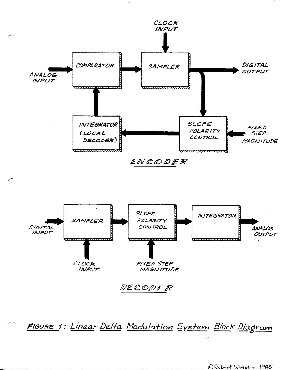
Most digital encoders sample the amplitude of a continuously varying signal at regular intervals and then represent these samples by binary words indicating their amplitude and polarity. In contrast, a delta modulator generates single-bit words whose value represents the quantized error, or "delta" (A), in a tracking signal rather than representing the value of the input signal itself. Technically, a delta modulator is a closed-loop sampled-data control system that produces a binary output whose polarity represents the difference between the input signal presently being sampled and a quantized approximation of the preceding input signal. This is accomplished by placing a comparator in the forward path and an integrator in the feedback path of a simple control loop. As shown in the Linear Delta Modulation System Block Diagram in Figure 1, the inputs to the comparator are the input signal and the output of the integrator, or local decoder.
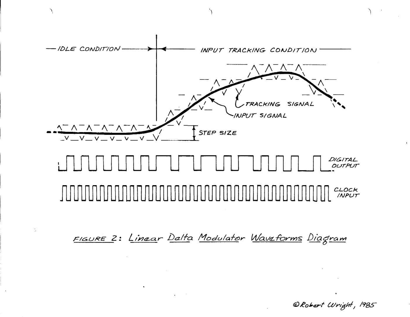
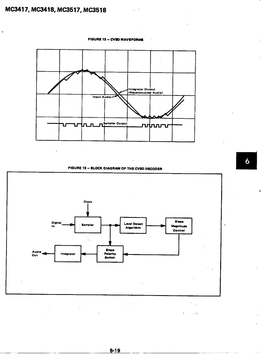
Thus the comparator output reflects the sign of the difference between the input signal and the integrator output. This sign bit controls the polarity of the charge next applied to the integrator and also forms the digital output. The comparator output is normally clocked so as to provide a synchronous band-limited serial digital bit stream. The simplicity of the required circuitry and the serial nature of the output data are the two fundamental advantages of the delta modulator. If the resulting clocked serial bit stream is then delivered to a similarly constructed receiving integrator as is also shown in Figure 1, the output of this decoding integrator will be a copy of the original transmitting control loop integrator output. There is no framing information contained in the synchronous serial data stream and the replication of the original input as represented by the bit stream from the encoder begins immediately upon this data being input to the decoder. The fidelity of this copy will depend in the largest measure upon the extent to which the transmitting integrator tracks the original input signal. As may be seen from the waveforms shown in Figure 2, a Linear Delta Modulator Waveforms Diagram, the encoder's feedback signal attempts to track the input signal in a series of ramped steps whose size is constant. Because the feedback signal from the local decoder consists of steps that are of a constant or nearly constant size formed by a linear network this type of delta modulation is called linear delta modulation. The presence of these incremental steps in the decoder output results in a quantizing noise signal referred to as granular noise. Low pass filtering at the receiver output will eliminate most of this noise signal if the clock rate of the bit stream is an octave or more above the bandwidth of the input signal. A further reduction in the level of this noise signal may be realized either by reducing the step size increasing the sampling frequency/ or both.
The major drawback of any linear modulation system is the relative inability of such simply contrived control loops to maintain an adequate signal-to-noise (s/n) ratio over a wide range of input signal power, i.e. they have a limited dynamic range. In speech recording, for example, the varying power levels encountered in the speech patterns of different individuals will result in significantly different s/n ratios.
In a delta modulation encoder, information about the instantaneous slope, or rate of change in amplitude, of the input signal is indicated by the sequential rate of occurrence of each of the binary or logical output levels. With a zero slope, constant amplitude signal present at the input as shown to the left side of Figure 2, the resulting tracking signal is a series of ramped steps each equal in level but of opposite polarity. This further results in an alternating zero-one sequence at the digital output which may thus be seen to indicate or correspond to periods of relative silence, or a constant amplitude level, in the input signal. Any deviation from this desired result during silent periods is referred to as the idle-channel noise and of course, will cause a non-zero signal to be output from the associated decoder.
As explained, an alternating sequence of ones and zeroes will be output as the result of the application of an input signal with a zero slope. But suppose the input signal slope should change so rapidly that the feedback signal (i.e. the encoder's integrator output) can no longer track the incoming signal. In this case, a stream of bits of constant polarity will result at the output. This condition is called slope overload, and when it occurs the output from the decoder may be quite different from the original signal. The degree of difference between the original signal and its replica is referred to as slope overload noise. Slope overload noise contributes more to the distortion of a replicated waveform than does granular or quantizing noise and so has a larger effect on the absolute waveform fidelity. Human listeners, however, find granular noise to be perceptually more noticeable and annoying in reproduced speech signals.
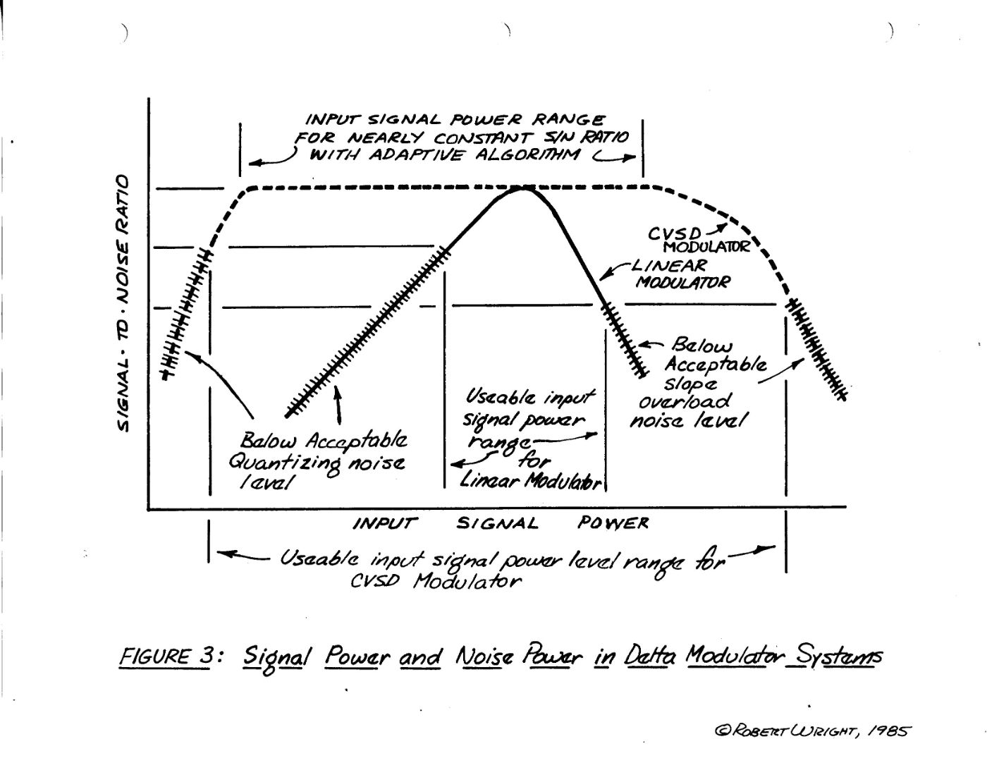
Thus we can see that the s/n ratio for a linear encoder is directly affected by the input signal power level. At a low input power level, the signal tracking is poor because the feedback tracking signal makes substantial excursions about the relatively small input signal and so the comparatively large step size generates significant amounts of granular noise. As the input signal power level increases, the s/n ratio improves linearly as the quantizing noise becomes an increasingly smaller part of the total power present. The ability of the encoder to track the input signal progressively improves until the encoder becomes slightly slope-overloaded. At this point, the s/n ratio begins to decrease as the noise power content increases more rapidly than the signal power content. A graphical representation of these relationships is depicted in Figure 3, Signal Power and Noise Power in Delta Modulator Systems.
The frequency limits for the analog input signal to the* encoder are bounded on the upper end. There is some clock frequency determined by the Nyquist sampling rate which is larger than the input signal bandwidth and which will encode the signal at a given noise level, provided we have a small enough step size. The amplitude limits for the input signal, however, are bounded at both the upper and lower ends. For any particular input signal level, there is an associated integrator step size which will provide the optimum s/n ratio. Unfortunately, the fixed step size results in a relatively small limiting value for the useful input signal dynamic range in a linear encoder.
Consider now the improvement in the s/n ratio which would result if the tracking step size could somehow be made small when the slope of the input signal is small, and then large when the slope becomes steep. This could be accomplished by adjusting the integrator's gain. Obviously, the feedback signal would then track better over a wider range of input power levels. Since the quantizing noise is proportional to the square of the step size, making the step size adaptable to a wider range of input signals would cause the noise power to vary with the input signal power instead of being independent of it as it is with linear delta modulation. Making the noise power proportional to the signal power therefore causes the s/n ratio to have a constant value independent of the input signal level. This is the principle of adaptive delta modulation. For a given clock rate and input signal bandwidth the approach of adjusting the integrator gain can provide a considerate increase in the useful dynamic range as is shown in Figure 3.
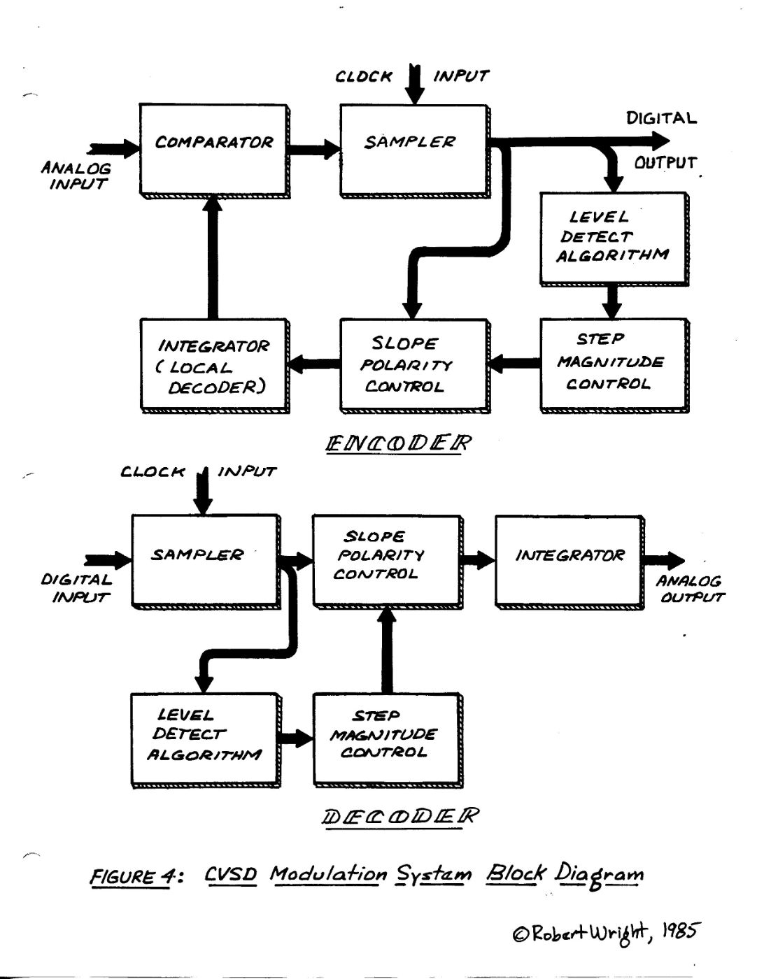
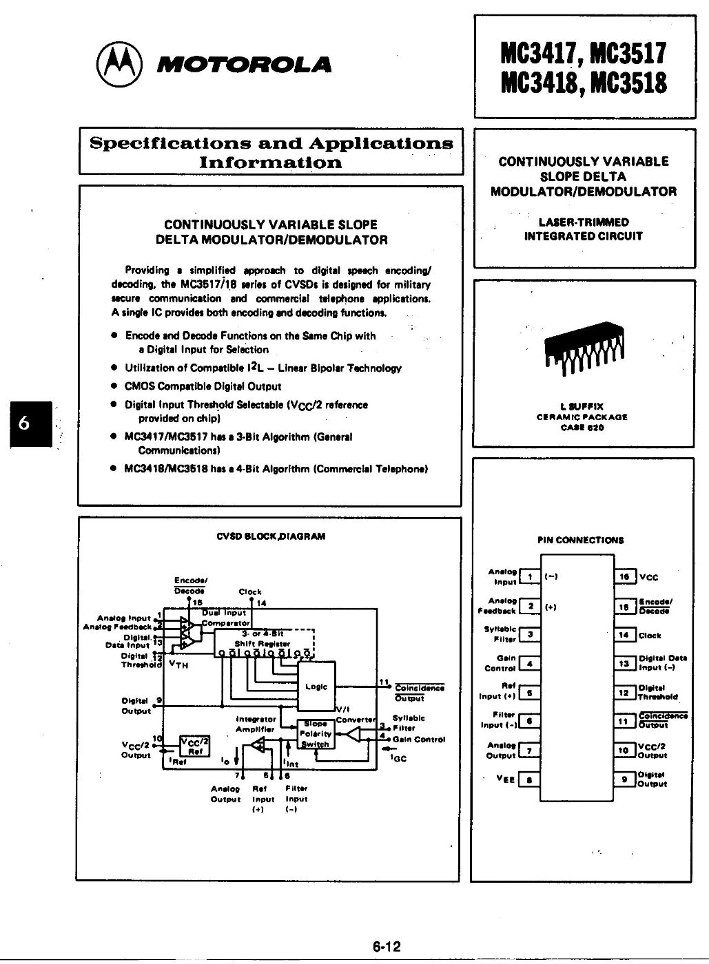
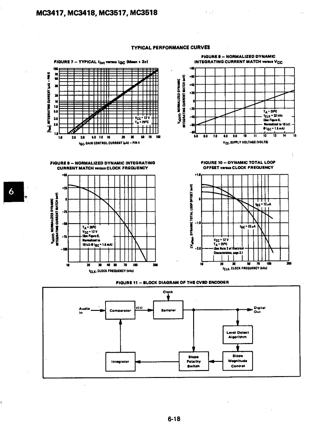
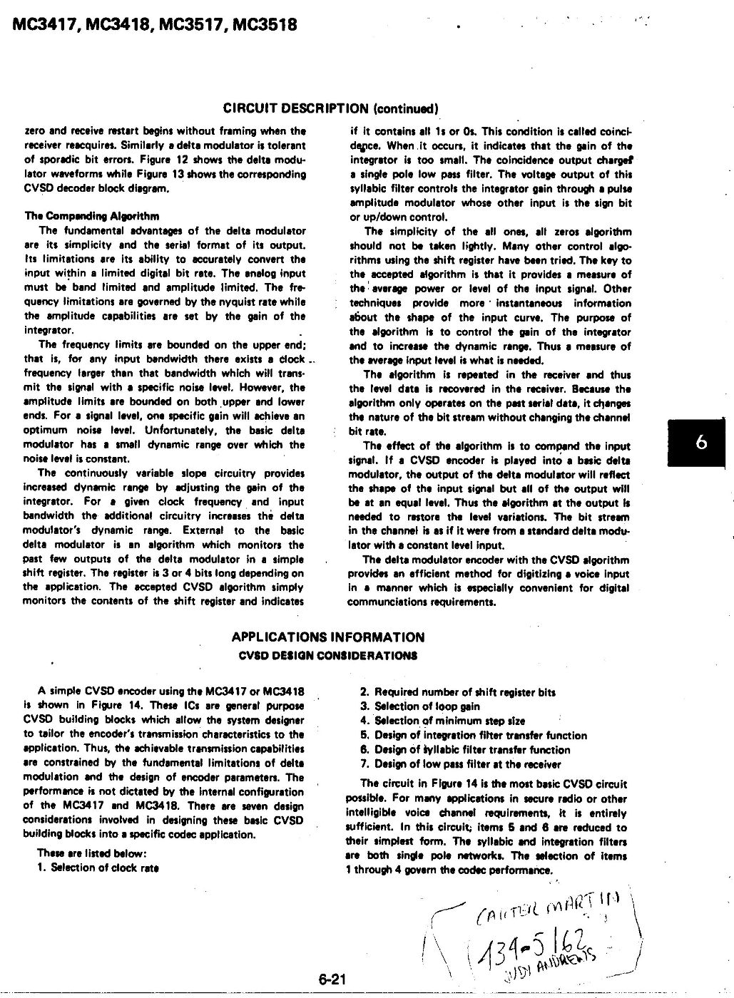
Many algorithms have been used to adaptively change the tracking integrator step size, but the Talking Box employs the technique known as continuously variable slope delta (CVSD) modulation. Also referred to as syllabically companded delta modulation, it is a preferred method for encoding and decoding speech or other analog signals having a large dynamic range. External to the operating elements contained in the linear delta modulator shown earlier is the implementation of an algorithm that monitors the present and past few digital outputs from the delta modulator and then adjusts the encoder integrator's gain accordingly. As is shown in the CVSD Modulation System Block Diagram, Figure 4, the monitoring part of the algorithm is realized with a simple shift register that stores the last three or four output bits. The accepted standard algorithm provides an indication when all of these sequentially stored bits are of the same logic level, a condition thus called coincidence. The occurrence of a true coincidence output signals that the present integrator gain is probably too small to track the analog input. The coincidence output allows a larger current to charge a low-pass filter, and the voltage output of this filter is then employed to adjust the absolute magnitude of the encoder integrator gain. Most applications use a simple single-pole low-pass filter with a fixed coincidence time constant ranging from about five to ten milliseconds, which is equivalent to the pitch period typical of voiced speech, up to about a hundred milliseconds, which is equivalent to the typical syllabic durations of speech. Hence this filter is often referred to as the syllabic filter in speech codec applications. Often the time constant value is ultimately selected as a matter of subjective preference.
This coincident sequence of logic levels detection algorithm is significant, both because of its elegant simplicity and because many other algorithms using the shift register have been tried with less satisfactory results. with the accepted algorithm the presence of the coincidence signal is related to the nature of the envelope of the input signal and so indicates of the signal's time-averaged power level rather than the more instantaneous information about the slope of the input curve that other sequence detection methods provide. The effect of the algorithm is to compand^the signal and thereby increase the realizable dynamic range.
The algorithm is repeated in the decoder and so the level data is recovered at the receive end. If the CVSO encoder data stream were input to a linear decoder, the essential shape of the encoder's analog input signal would be replicated but all of the output would have equal levels. The bit stream appears as though it were coming from a linear encoder with a constant input level, and so the algorithm is required at the decoder end to restore the amplitude level variations by decompanding, or expanding, the signal. It is interesting to note that since the algorithm operates only on the past serial data, it is effectively equivalent to increasing the information content of the bit stream without changing the channel bit rate.
So we may see that the principle of delta modulation coupled with the CVSO algorithm provides an easy-to-implement, efficient method for digitizing voice frequency analog information into a serial data stream.
Specifics of the Talking Box Circuit Realization
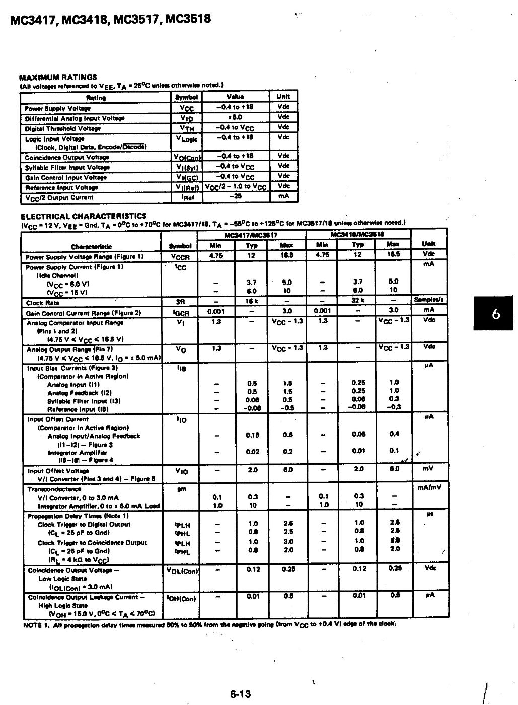
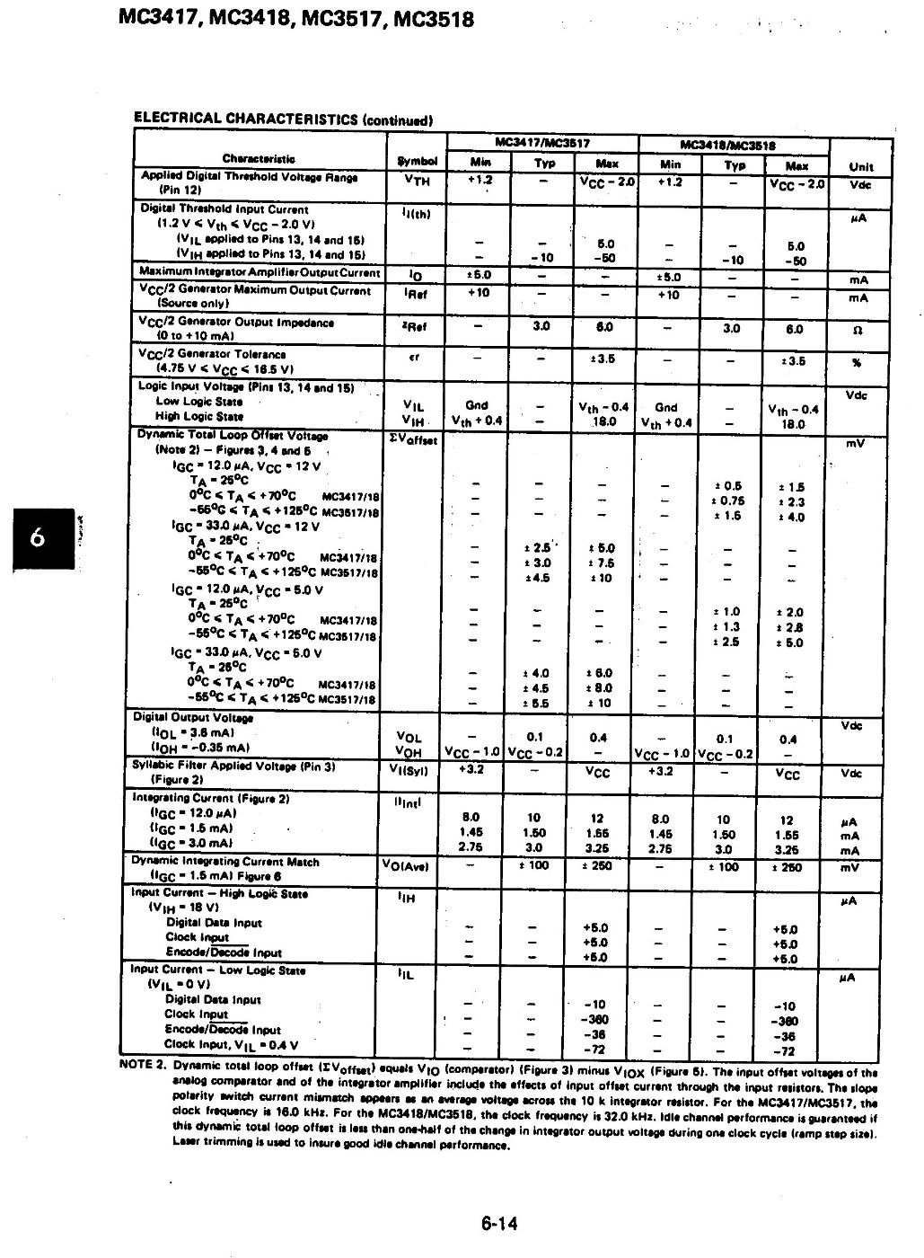
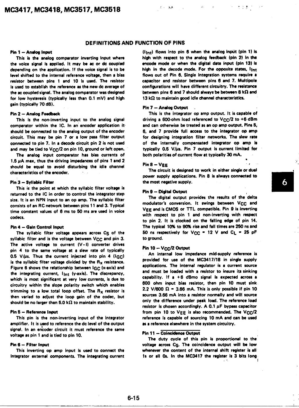
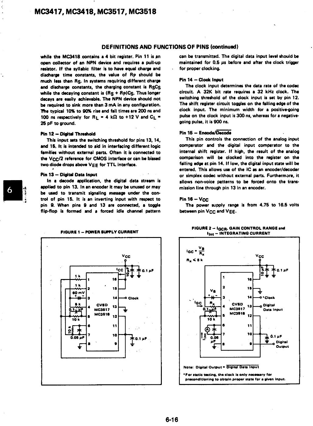
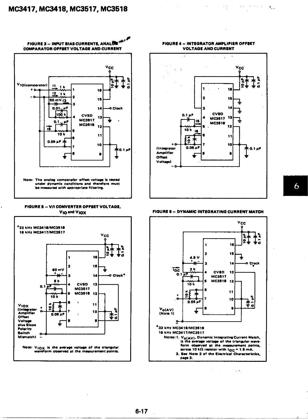
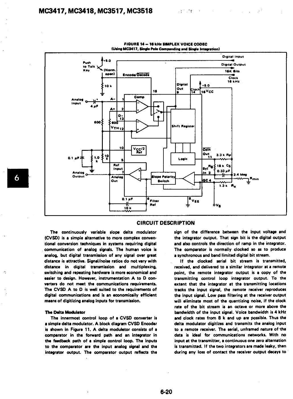
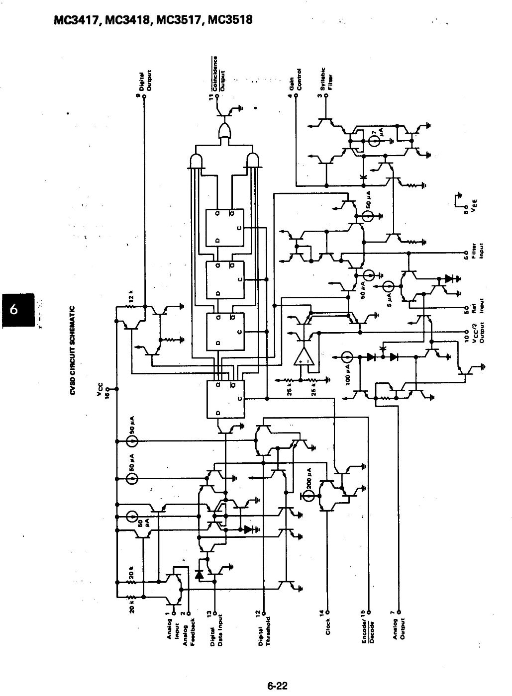
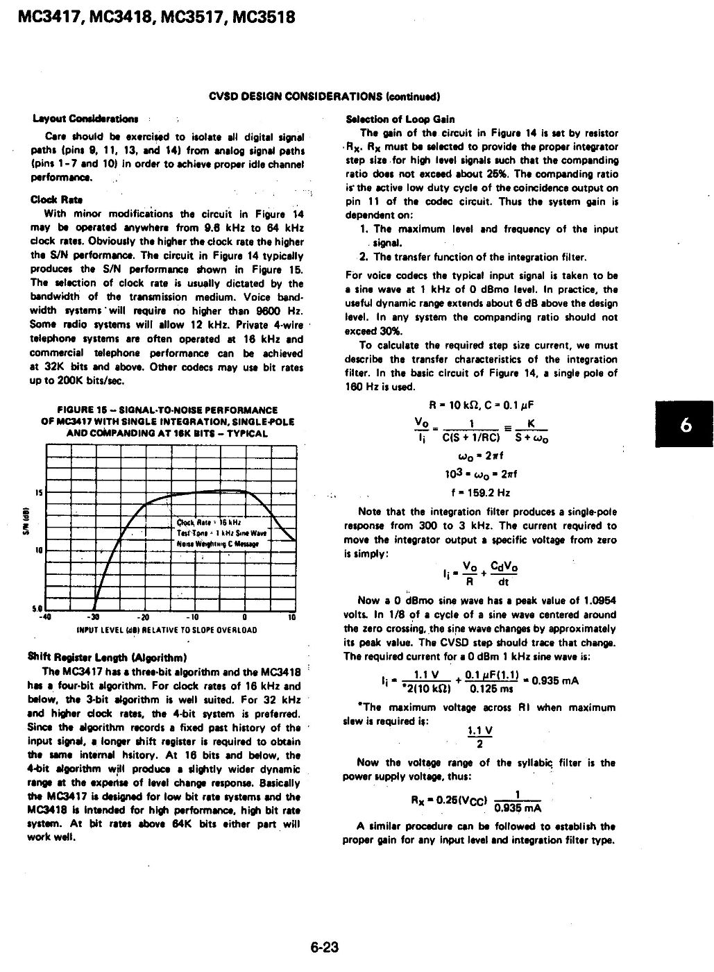
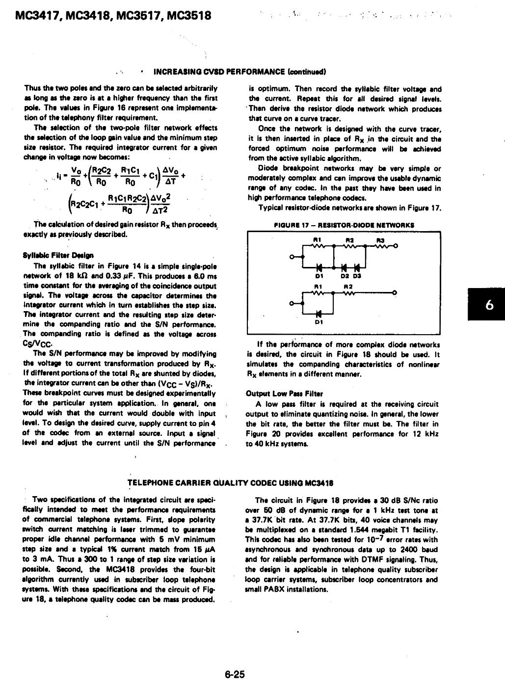
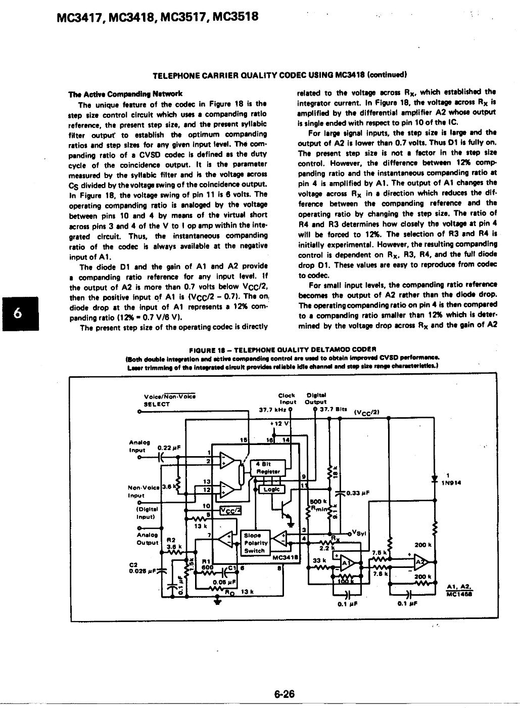
The Talking Box implements the CVSD encoder and decoder electronic circuitry using the Motorola MC3417 or MC3418 integrated circuit (IC) to accomplish the delta modulator functions. These ICs are general-purpose CVSO building blocks that allow the circuit realization to be tailored to the particular requirements of an application. According to Motorola, current matching for the slope polarity switch is laser trimmed during the MC3418 IC's fabrication to guarantee idle channel performance with a five-millivolt minimum step size and a typical one percent current match from fifteen microamps to three milliamps. This allows a step size variation of three hundred to one, which reflects the capability for a significant analog signal dynamic range.
Since the Talking Box circuitry itself consists of a separate encoder and decoder path this allows for their simultaneous use to both send and receive, permitting full duplex operation. Both the encoder and the decoder are driven by the same variable rate TTL clock generator circuit. Support elements consisting of a pair of voltage regulators and the RS232 interface level converter ICs are the only other parts on the printed circuit card.
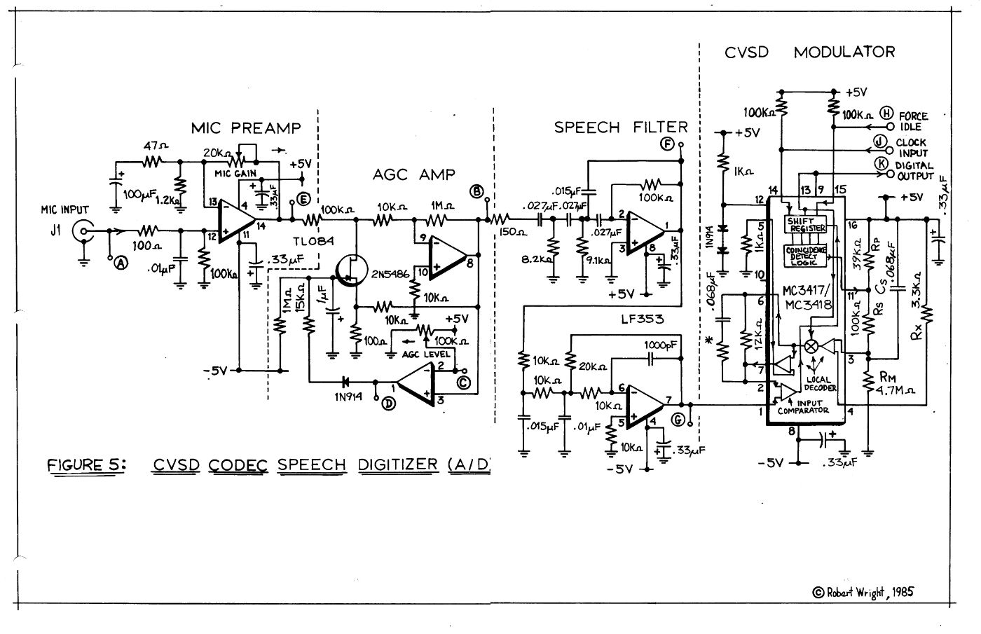
The encoder path electronic circuitry is shown in the schematic diagram of Figure 5, a CVSD Codec Speech Digitizer (A/D). As is shown there, the circuit is divided into four functional areas, beginning with the microphone preamplifier circuitry, followed by an automatic gain control (AGC) amplifier, a speech bandpass filter, and finally ending with the CVSD modulator circuit itself.
The microphone preamplifier is a classic transformerless unbalanced, or single-ended, input amplifier circuit. For optimum noise performance with the low-level signals expected from an audio source such as a dynamic microphone, the design uses a noninverting configuration. This implementation is realized in one-fourth of a TL084 type quad operational amplifier (op amp) IC with high impedance field effect transistor (FET) inputs. The preamplifier has an adjustable gain that can be varied by using a trimpot which is connected as the feedback resistor, labeled MIC GAIN. The amplifier also has a low-frequency roll-off, i.e. high pass characteristic, whose corner frequency is established by the values of the series resistor/capacitor combination going from the inverting input of the op-amp to the ground. This serves to reduce the ambient AC field (usually 60 Hz) hum pickup sensitivity of the preamplifier and to reduce the low-frequency power content of the input signal. Finally, the preamp also has a small value capacitor placed from the noninverting, or signal, input of the op-amp to the ground which serves to bypass undesirable high-frequency noise that may be present on the microphone cable. Note that the series input resistor (100 Ohms) may be replaced by a capacitor, usually of about one microfarad, for some applications.
Following the microphone preamplifier is an A6C amplifier circuit which serves to provide level compression of the audio signal before applying it to the speech filter and CVSD codec. This action limits the dynamic range of the signal amplitude previous to its submission to frequency bandpass and encoder processing. The AGO circuit employed in the Talking Box is one described by Jerald Graeme of Burr-Brown Research Corporation*. Its operation is based on the use of an FET as a controlled variable resistance element in a tee voltage divider network which determines the gain range and output amplitude of this stage.
The AGC circuit action is realized with the FET and two op amps from the same quad package partly used for the microphone preamplifier already described. The first op amp serves as a gain-controlled inverting amplifier, and the second as a peak sensing amplifier. If the peak positive level of the output signal exceeds the voltage value set at the wiper arm of the AGC LEVEL potentiometer then the output of the sensing comparator will swing positive, increasing the FET's gate voltage and thus lowering its dr in-to-source resistance. This in turn will cause more of the input signal to be shunted to the ground, ultimately resulting in reduced overall circuit gain for this stage. The output signal amplitude may be set from between zero to the saturation or clipping level of the gain-controlled amplifier by adjusting the AGC LEVEL control potentiometer just mentioned above»
A difficulty encountered with many implementations using the concept of a FET as a variable resistance element for audio signals centers on the fact that the resistance of the device itself is modulated by the signal impressed across it. Failure to adequately compensate for this aspect of the FET's characteristics will result in signal level-dependent gain and distortion. The circuit shown in Figure 5 employs a novel correcting feedback method to significantly reduce this signal level modulation. As may be seen, the signal appearing at the FET's drain lead is matched by an equal but opposite in-phase signal derived from the output of the associated AGC amplifier. The resistance values used in the circuit are selected so as to allow the FET to enjoy operation at small-signal levels; a circumstance which also aids to minimize distortion. As shown, the output of the AGC stage is then applied to the speech bandpass filter next seen in the encoder's signal path.
The speech bandpass filter circuit stage nominally allows input signals within a frequency passband of from 300 to 3000 Hz to pass through while rejecting those that lie outside of this range. One of the major considerations in the selection of an implementation technique for bandpass filters is the value of a derived parameter referred to as the normalized or fractional bandwidth. Numerically, it is the result derived by subtracting the lower -3dB, or half-power, cutoff frequency from the upper -3dB cutoff frequency and further dividing this difference value by the geometric mean of these same two frequencies. The. geometric mean is of course the square root of this just computed difference value. The fractional bandwidth thus calculated from the encoder speech filter's specified (high and low) cutoff frequencies has a value of approximately three, we find that as this calculated value for the fractional bandwidth begins to pass a value of about 0.8 and approaches or exceeds unity (or a numeric value of one) from below, generally better results for the bandpass filter performance are realized from cascaded high- pass and low-pass filter sections rather than from a true bandpass implementation. This is the method used in the encoder speech filter circuit.
Another area of consideration is the need for good frequency and transient response characteristics for the speech, filter. The Butterworth type of filter has the flattest passband amplitude while providing a moderately fast initial attenuation rolloff rate. Although there is a phase shift with frequency change across the passband when using these filters, it is gradual and is not audibly perceptible. Additionally, this kind of filter has a low amount of overshoot and an acceptable transient response. All of these factors combine to provide low signal distortion with this variety of filters. The high and low pass filter types chosen for use in the encoder are third-order active filters which exhibit a sharp cutoff rate of -18dB per octave beyond the corner frequency and a flat power and voltage frequency response with a gradual change in phase shift across the band. The particular electronic circuit employed to implement the filters is referred to as an infinite-gain # multiple-feedback design and was chosen because it offers a good compromise between complexity and component value spread and sensitivity. Each section is realized with one-half of an LM353 dual FET input op amp IC. These devices have a very high input impedance, a fast slew rate, and extremely stable operation with capacitive loads. Because there are two inverting op amps cascaded in the filter, the net result approximates a zero phase change through the stage.
The output signal from the speech bandpass filter is then finally applied to the CVSD modulator circuit. Essentially all of the active functionality of this stage is contained within the IC itself while the discrete components serve to establish the particular parameters of three areas of the device operation.
First, we find that two silicon diodes are connected from pin 12 of the IC to the ground which establishes the threshold point for the logic signal inputs to the device at approximately 1.4 volts (about two diode drops) above ground for use with TTL logic levels or the RS232 interface ICS also on the board.
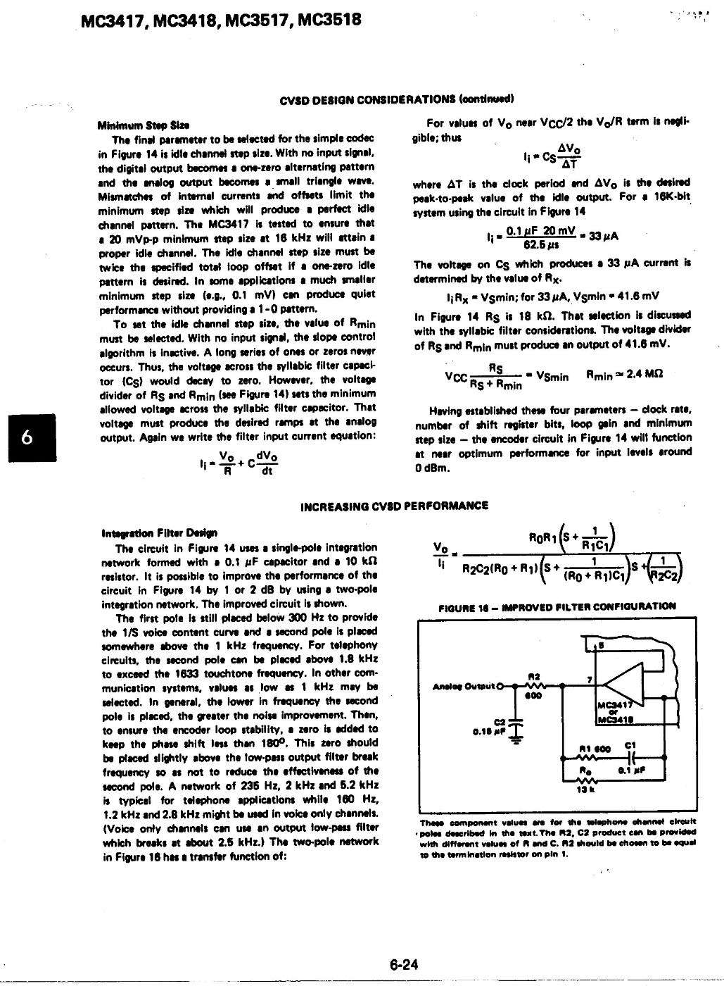
The second area of consideration is the tracking integrator filter network. The Talking Box circuit uses a single-pole integrating filter network connected across the local decoder integrator amplifier between pins 6 and 7 of the IC. The output
of the tracking integrator appearing at pin 7 is also connected to one input of the analog signal comparator at pin 2. The use of a two-pole network for this filter can improve the s/n ratio by one or two dB over the single-pole realization. If desired a two-pole network may be implemented by cutting the trace connecting pins 2 and 7 on the top of the printed circuit card and jumpering the pins on the conductor side with a suitable resistor, and then adding a capacitor from pin 2 to ground. Derivation of the necessary component values is explained in the Motorola data sheet 2.
Note, however, that the single pole filter shown and ordinarily used has proven entirely adequate for TouchTone reproduction at a 32 kbps data rate with the MC3417 device.
The final area of the CVSD modulator operation is the syllabic filter network and the determination of the integrator minimum step size and loop gain for the IC device. The syllabic filter is a simple single-pole low-pass circuit that consists of the two resistors labeled Rs and Rp, and the capacitor Cs. Normally the capacitor is charged through Rs and Rp in series. But when the coincidence output, pin 11 of the IC, becomes true this acts to effectively remove the upper resistor, Rp, from the charge path for Cs and thus increases the charge current and ultimately the integrator step size as a result. The resistor Rm serves to determine the minimum integrator step size while the value of resistor Rx serves to establish the loop gain by a simple linear current-to-voltage transformation. Modifying this transformation relationship can result in a significant increase in the s/n ratio but with an attendant increase in electronic circuit complexity. For example, the use of active circuit devices to accomplish this function can easily result in 50 dB of useful signal amplitude (dynamic) range with a 30 dB s/n ratio when operated at a 32 kbps data rate.
There are three digital or logic-level signal paths associated with the operation of the CVSD encoder IC. The first of these signals is the clock input to pin 14, which is ordinarily provided by the clock generator circuit described below. A second logic signal is the digital output appearing on pin 9, which is the actual serial data stream coming from the modulator. The data bits are clocked out of the device on the falling edge of the clock input to the IC at pin 14. The third and final logic signal is the force idle input, IC pin 15, to the circuit. When the digital output from pin 9 is connected to pin 13 of the IC as is shown, a toggle flip-flop is formed within the device, and making the force idle input pin active then results in the transmission of an idle channel pattern from the encoder digital output. This feature allows for an easy way to establish data link synchronization or to force a silence pattern from the encoder.
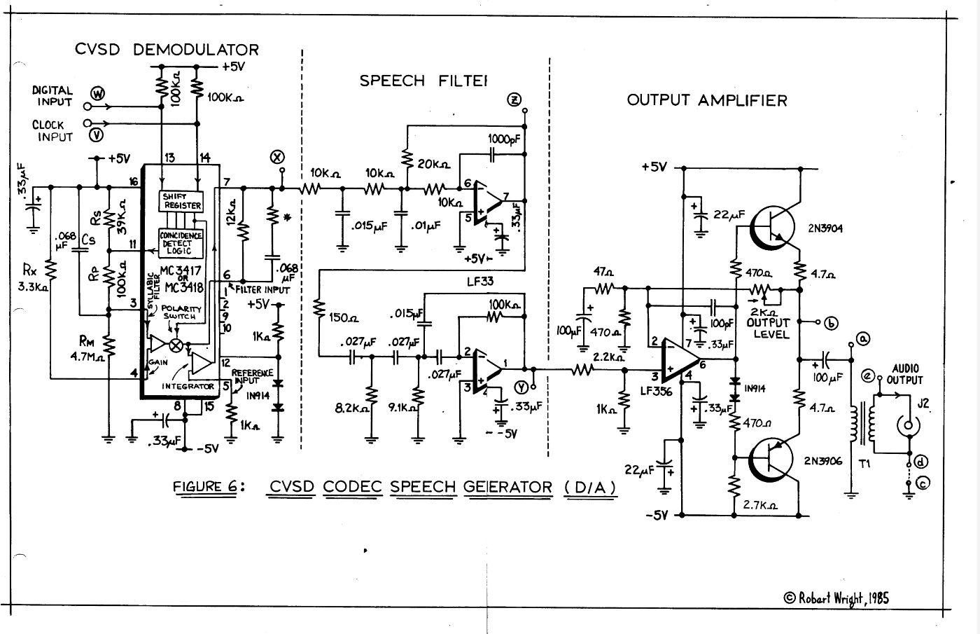
Having thus examined the particulars of the circuitry comprising the encoder path for the Talking Box, let us now turn our attention to the circuit design used in the decoder path. The schematic diagram for the entire decoder path is shown in Figure 6, a CVSD Codec Speech Generator (D/A). As may be seen from this diagram, the decoder path consists of three main stages of operation, beginning with the CVSD demodulator, followed by a speech bandpass filter whose output finally drives an output amplifier.
As was explained in the section on the principles of delta modulation, the decoder function may be seen and understood as somewhat complementary to that of the encoder. Not surprisingly then, we may note a mirrored similarity in their respective electronic circuits and component values.
Thus in the schematic for the CVSD demodulator stage the operating function and value for the resistors labeled Rp and Rs together with the capacitor Cs is entirely analogous to the operating function and value of those identically labeled components in Figure 5, the diagram for the encoder path circuit. Similarly, the resistors labeled Rx and Rm serve in a manner analogous to that of their identically labeled compliments in the encoder implementation. In a similar fashion, even the components forming the decoder integrator filter network for the CVSD demodulator are analogous to those found in the modulator circuit. Finally, the logic threshold levels for the decoder IC are also set by the drop across a pair of silicon diodes as is done with the encoder IC.
In the decoder path, however, there are only two digital signal paths associated with the circuit. There is a clock input which is ordinarily driven by the same TTL clock generator circuit used for the encode function. This signal is applied to pin 14 of the decoder IC and clocks the data bits then appearing each in turn on the digital input, pin 13, into the IC.
The output o£ the CVSD demodulator stage is of course an unfiltered copy of the original analog signal which was once input to the encoder path. It is then next applied to the decoder path speech bandpass filter which serves to remove the granular or quantizing noise described earlier. The hardware realization is essentially identical to that employed in the encoder path save that the cascading order of the high-pass and low-pass circuits has been reversed. In the decoder filter, the first object is to remove the quantizing noise as much as possible, thus the low-pass function is placed first and closest to the input of the filter stage (and so to the decoder output as well) to maximize this attenuation.
Shown following the speech filter in the decoder signal path is the third and final decoder circuit, the output amplifier. As the name implies, this stage amplifies the audio signal which is output from the speech filter. A pair of complimentary silicon bipolar transistors are connected as buffer devices to improve the power output capability of the LF356 op amp IC used in this circuit. A gain (or OUTPUT LEVEL) control is provided in the form of a trimpot in the feedback path, but the value of the resistor going from the noninverting input of the op amp IC to ground may also be modified to adjust the range of the output level. Ultimately the amplified signal is coupled through a large valued electrolytic capacitor to the primary of the output transformer. The signal developed across the secondary is then the final output of the decoder path, which completes the description of this portion of the electronic circuits.
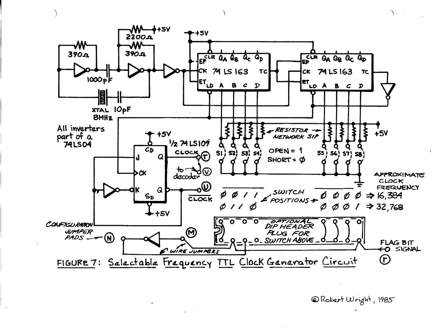
As was mentioned previously, in addition to the encoder path and decoder path circuits just described, the other major circuit element of the Talking Box is the clock generator used to control the timing of these first two. The schematic diagram for this circuit is shown in Figure 7, a Selectable Frequency TTL Clock Generator Circuit. As may be seen there, this circuit consists essentially of a crystal-controlled oscillator driving a programmable divider chain whose divide modulus is determined by the value set on an associated dipswitch. The programmable divider is thus very easily configured for a large range of data clock rates, and in fact, for flexibility, this clock rate may be arranged to be selectable by the associated computer through the connecting interface.
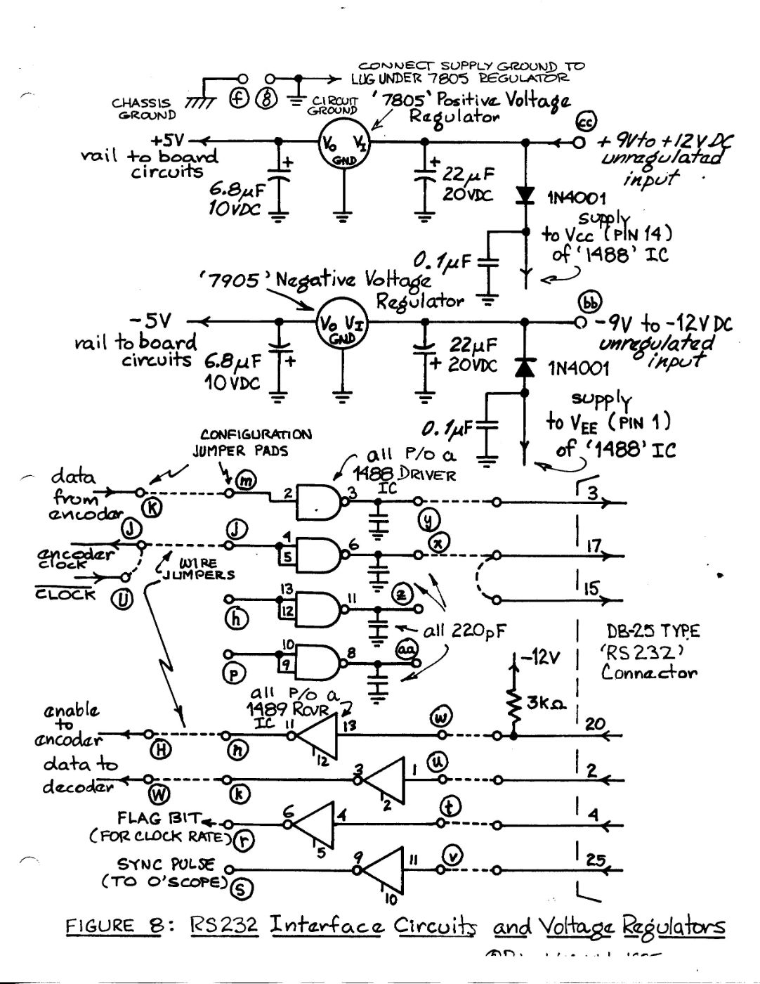
The final electronic circuit components on the printed circuit board are the support elements consisting of the positive and negative voltage regulators and the RS232 level converter ICs used by the computer interface. A schematic drawing including these parts is shown in Figure B, the RS232 Interface Circuits and Voltage Regulators diagram.
Having thus seen how delta modulators work in general and then further how this one in particular operates, let us now see how the actual hardware is realized and physically constructed.
The Talking Box Project Physical Construction
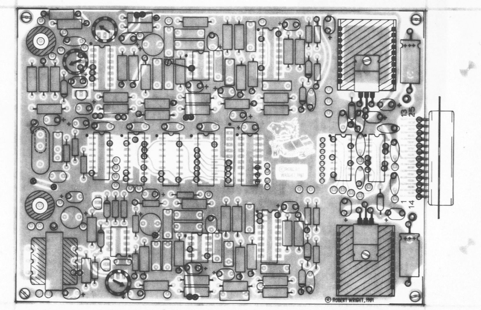
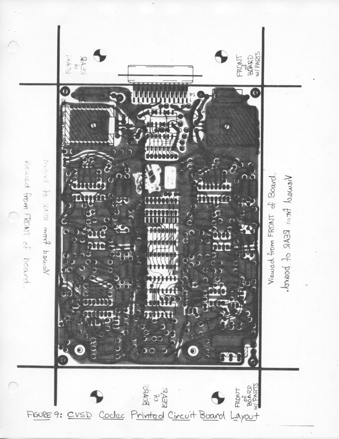
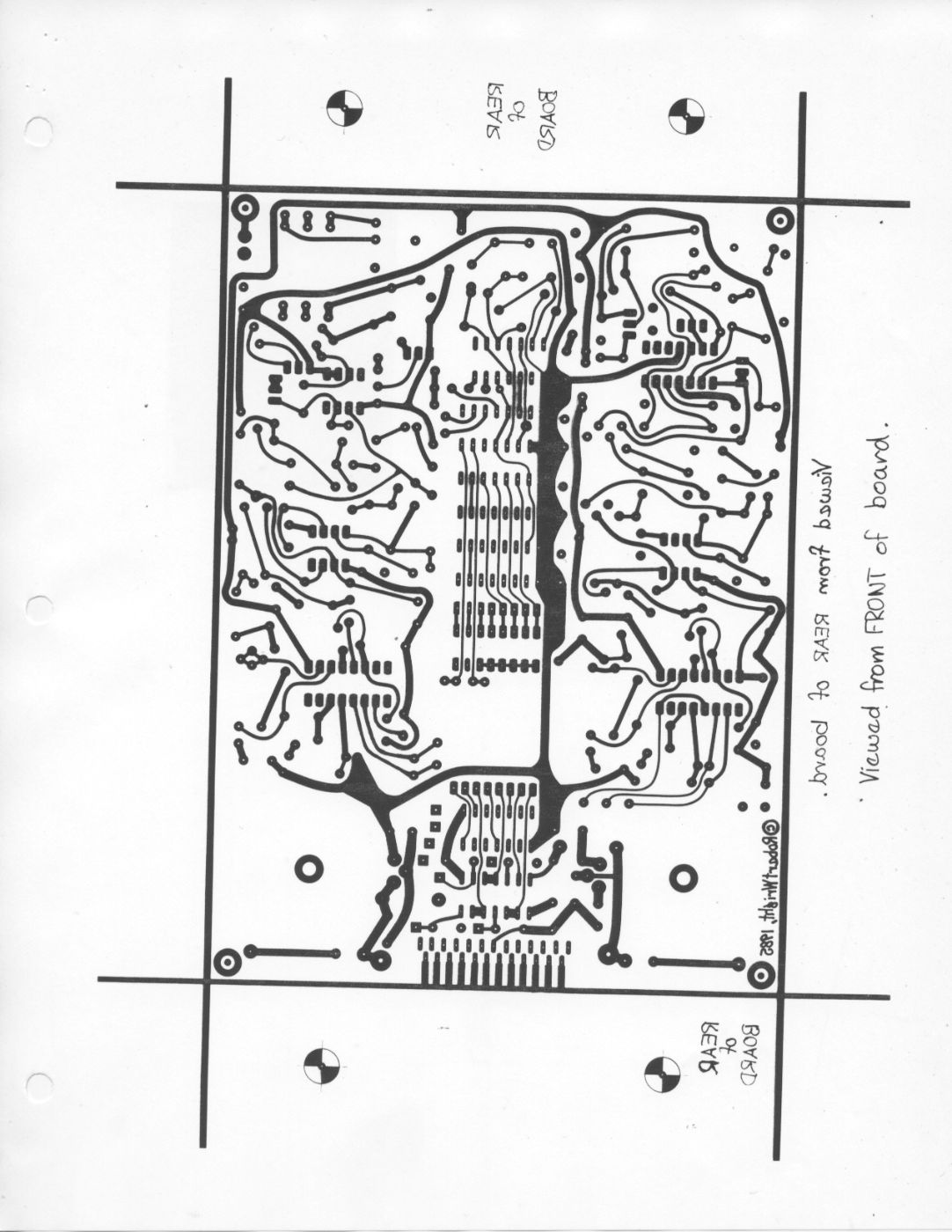
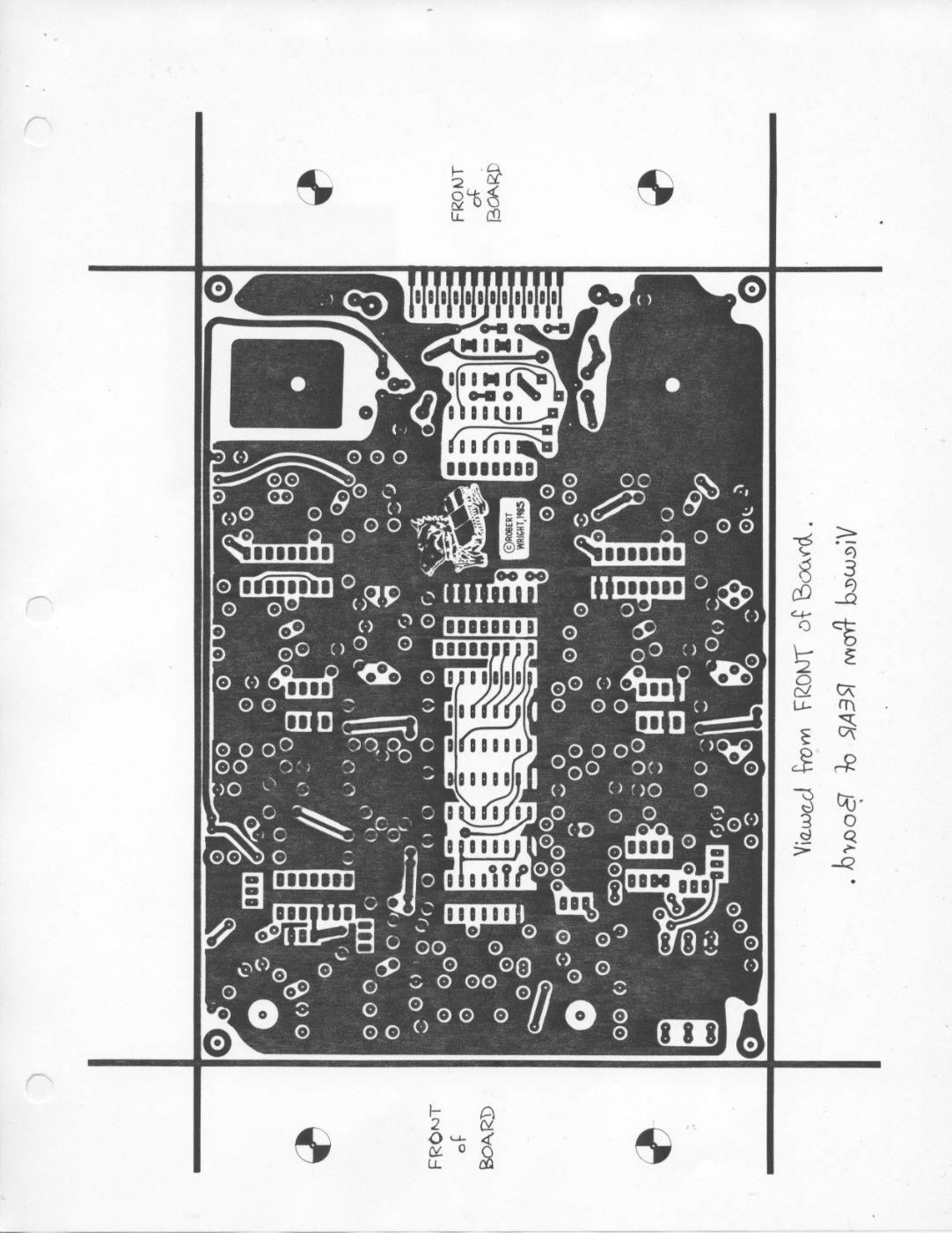
The electronic circuitry just described is all contained on a single double-sided printed circuit board. One side of this board is primarily used as a ground plane which allows the close placement and intermix of digital and analog circuitry. A positive image of the circuit traces on both sides of the printed wiring board is shown in Figure 9, the CVSD Codec Printed Circuit Board Layout. Observe that while the card is double-sided, or has conducting paths on both the front and back sides of the board, the layout is such that it does not require the use of plated through, or conducting, holes to connect the two sides. This is of course done to allow for an easy and inexpensive experimenter duplication of the circuit board suggested for use in the project. Finished circuit boards with plated through holes and film copies of the artwork are available as shown in the parts list.
Notice that alignment targets are provided on the peripheral areas at the sides of both the front and rear circuit layouts themselves. First, lift this artwork as a film image for each side (usually as a negative) being sure to include these targets in each case. Then, using these targets, align the front and rear film images atop one another and affix them in place to each other. Now punch three separate registration holes through both of the film sheets simultaneously with a round paper punch. Be careful to punch in a location outside of the areas of circuit artwork. The presence of these registration holes will then serve to allow the front and back film sheets to be aligned with one another by means of suitable pins placed through these holes while a piece of circuit board material to be exposed is placed between them in a sandwich like fashion, thereby ensuring easy front-to-back registration of the two sides of the circuit card. Such registration pins, precision sized, are commercially available from printed circuit supply houses, but experience shows that a pencil or dowel shaved to size will do nicely for this purpose if something like a preformed rod of the proper size is not available. A number 68 drill size is adequate for most of the supported holes, i.e. those which have a component lead passing through them. The exceptions are the regulator mounting holes which are number 37, and the phono connector mounting holes which are 3/16 inch diameter.
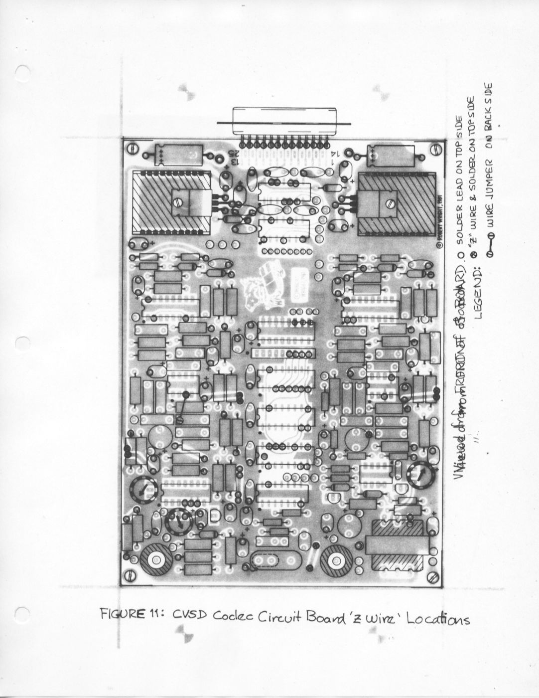
Two diagrams are used to show the component mounting and assembly details for the printed circuit board. The first of these, Figure 10, the CVSD Codec Circuit Board Component Assembly Diagram, shows the placement of the parts as they are to be mounted and soldered to the board and it also shows the location of various labeled points in the schematics, some of these labeled circuit locations serve as connections to use as test points while others are to allow for strapping various configuration options.
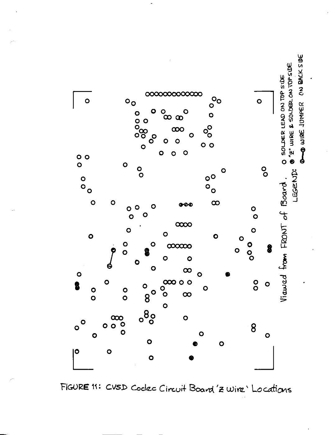
The second diagram. Figure 11, the CVSD Codec Circuit Board 'Z Wire' Locations diagram, details the location of those holes in the circuit board that must be soldered on the top or component side of the card. Note that this step is necessary only if there are no plated-through holes on the board and that the board shown in the parts list has such holes. If there is a component lead in this hole location, then solder it on both sides of the board. If there is no component lead through this hole, pass a wire lead through the hole and the clinch and solder it to the board on both sides. This method of achieving a conductive via or path from one side of a circuit board to another is often referred to as a ”Z wire" because of the jumper's rude appearance to that letter, hence the title of Figure 11. Notice that none of the holes that thus must be soldered on the conductor side of the circuit board are blind, i.e. inaccessible with the components mounted. This allows the project circuitry to be easily assembled with a homebrew printed board requiring no plated through holes and very few jumpers.
The RS232 connector itself is to have the upper row of pins, i.e. numbers one through thirteen, soldered to on the top or component side of the board while the bottom row, pins twelve through twenty-f ive, is to be soldered to on the back side of the board.
Computer Interface Operation for the Talking Box Project
Now that we have seen the electronic principles of CVSD operation and how the project circuit board is physically constructed, the next area we will examine is the software needed to interface the device to an associated computer.
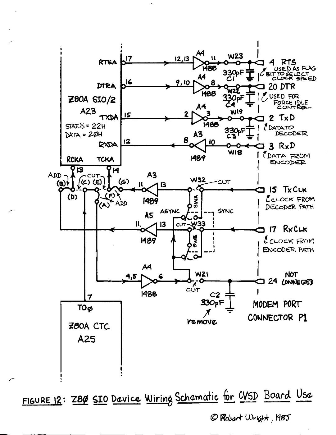
As was mentioned in the introduction, the Talking Box appears essentially as though it were a synchronous modem to the connected supporting computer. We have described five digital signal paths into and out of the project circuitry thus far. These were of course the two data paths, one to the decoder and one from the encoder; the two associated clock signals; and the force idle input to the encoder. Some other optional physical interface signals are described in the next section on application examples. However, since the immediately following explanations are concerned only with the programmatic aspects of the data exchange operation itself, just these five signal lines are now assumed to be connected to and from a serial I/O port on an associated computer. The hardware specifics of this interconnection are shown in detail in Figure 12, the SIO Device Wiring Schematics for CVSD Board Use.
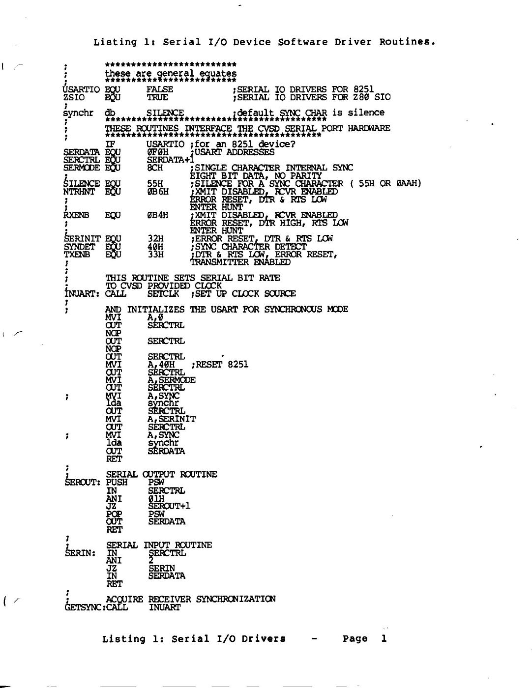
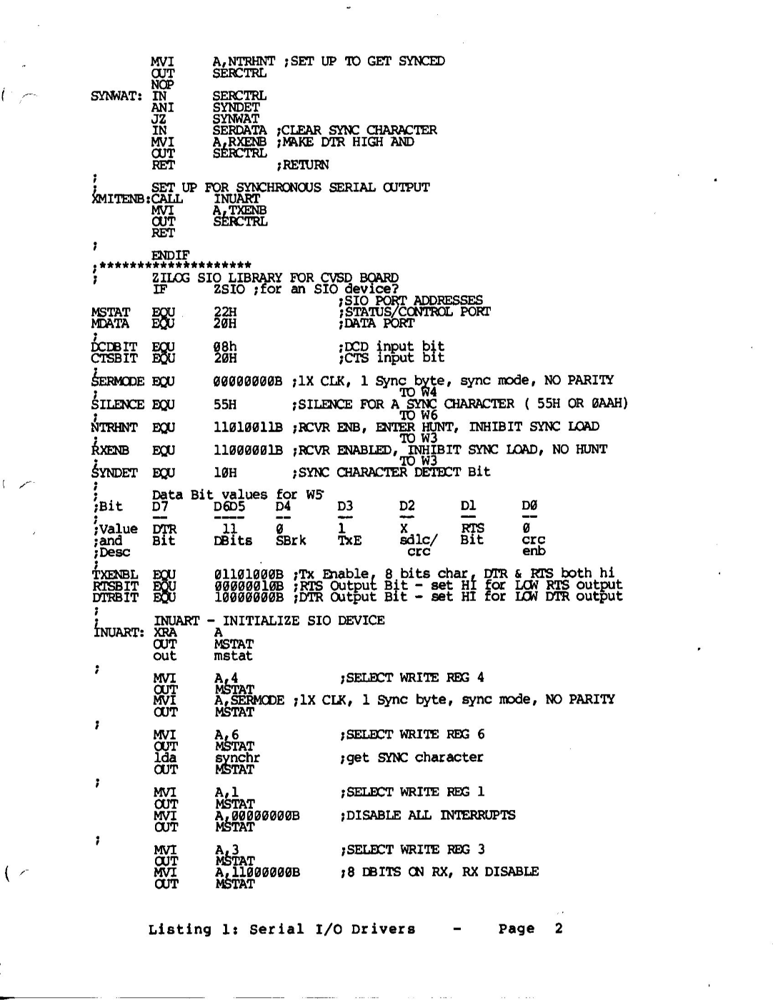
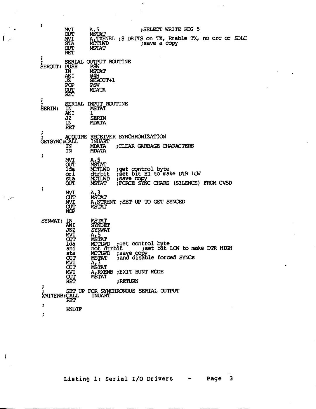
In the course of the following discussion, we will refer to the software routines shown in Listing 1, entitled a CVSD Driver Program. This program listing contains both that module of routines necessary to control an Intel 8251 compatible serial I/O device, i.e. USART, and that module needed to control a Zilog SIO compatible serial I/O device. With the appropriate choice of driver module, either of these devices may easily be operated in a synchronous mode suitable to the requirements of the Talking Box. The source code is written entirely in Intel 8080 assembly language and the choice of use between modules is made by equate statements.
Both the USART and the SIO software driver modules each contain four main routines, or entry points, which are directly concerned with the computer's exchange of data with the encoder/decoder. These four entry points are the INUART routine, the SERIN and SEROUT routines, and the GETSYNC routine.
Before its first use to transfer data in either direction, the user must first initialize, or software configure, the serial I/O device itself to operate in a synchronous mode. This is accomplished by a call to the routine labeled INUART. In either module this instruction sequence essentially serves to load the control registers of the I/O device so that we cause it to operate on eight-bit (byte-wide) data characters with no parity bit added, and so that it will use a single character as a template for a pattern to match within the serial bit stream (often called the SYNC character) to assume that synchronization on a character boundary has been encountered (called sync detect).
Notice that in most synchronous communications there are no character framing bits such as the start and stop bits familiar to asynchronous, or character-oriented, serial communications protocols. instead, each bit forming a character is in turn transferred into or out of the serial device by a timing signal presented on a separate signal connector path and the character boundaries are determined by counting off the appropriately defined number of bits per character from the clocked in bit stream. Most "real", or synchronous telephone modem, data transfer applications send and receive the data characters in blocks with pauses between these transfers for periodic resynchronizations of the data stream and to allow for such things as error checking the contents of each block. For obvious reasons then, synchronous methods are often called message-oriented serial communications protocols.
Once either the SIO or the USART device is initialized and then set into operation, they both continue to be relatively easy to control in software. In both cases, the SERIN (get a character from the port) and the SEROUT (output a character to the port) routines are the same as they might be for a simple asynchronous application. Thus the character input and output routines involve only the looping test of a bit level within a status byte which is read in repeatedly from the I/O device in order to determine whether a character is ready to be accepted or delivered. When this test is finally satisfied the character itself is then actually read from or written to the serial port before the routine is exited with a return to the caller.
The remaining driver routine is that one labeled GETSYNC. Once again the routine accomplishes much the same function for either choice of I/O device. This entry point is usually called at the beginning of a record cycle to actually start the input of audio data from the encoder. In this task, the routine first serves to hold the force idle input to the encoder true, thereby causing the encoder to generate the same alternating one-zero bit sequence output that represents silence, until the serial I/O device then detects the string of such bits as a match for the synchronizing character. When the test for the presence of this character is satisfied, the force idle signal line is immediately returned false, allowing the encoder to begin sending audio data to the serial port which is then next set to receive this data before the routine is finally exited. Notice that for some applications the value of this bit pattern used, i.e. the sync character, may be changed to then allow the start of audio recording on the hardware detection of a matching sequence corresponding to a certain place in a signal waveform for example.
These four hardware driver primitive routines are called upon by an application program to accomplish the task of physically transferring the audio data into and out of the computer. In the following section are some examples of applications using these routines with the project board and a supporting computer.
Some Specific Applications Examples
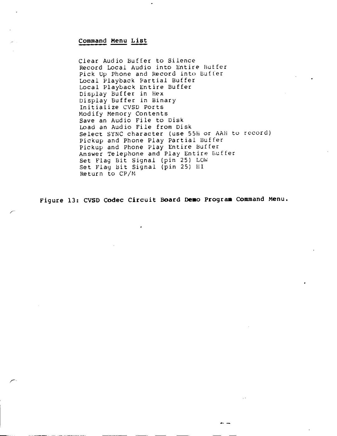
The Talking Box demonstration program used by the author employs these driver routines just described and allows for the selective execution of tasks from the menu of commands shown in Figure 13, the CVSD Codec Circuit Board Demo Program Command Menu. The program runs under the CP/M Operating System and has been tested on both an 8080 (homebrew) and a Z80-based (Televideo TS802H) microcomputer system. The assembly source code for this program is shown in Listing 2, the CVSD Codec Circuit Board Demo Program. [-optional inclusion]
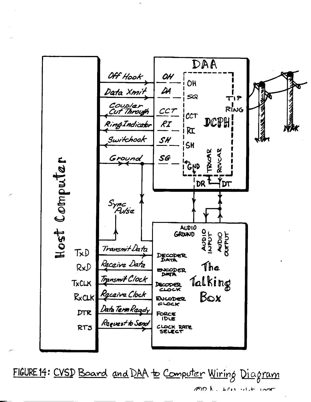
As may be seen from this table of commands, the program is set up to allow the operator to record and play audio from either the local microphone and speaker pair or from the telephone line. The interconnect arrangement used to attach the demonstration program and computer with the Talking Box to the switched telephone network is based on a device called a Data Access Arrangement or DAA. The particular device used by the author is an older (1976 vintage) Bell Telephone Type 1001F Data Coupler, although newer FCC Part 68 registered hybrid modules that duplicate its DAA function may be had for somewhat less than twenty dollars from such firms as Cermetek (CH1810 Direct Connect Protective Hybrid, or DCPH, see references). These modules provide identically functional connections, but they are significantly smaller in size and much improved in the convenience of use, being intended to mount inside a device instead of hanging on the wall in a separate enclosure! Notice that the DCPH modules employ CMOS logic level signal paths whereas the DAA has RS232 signal level requirements. Either the DAA or DCPH can provide an indication that the telephone is ringing and allow the computer to control the device's onhook/offhook (or answer/hangup) status and control its application or reception of audio to and from the phone line. Both provide a so-called billing delay timer, signal overload protection, line isolation, and protection and the ability to seize and dial pulse the telephone line, i.e. call out. The physical wiring used to connect the DAA or DPCH and the Talking Box to the host computer is shown in Figure 14, a CVSD Board and DAA to Computer Wiring Diagram.
In addition to allowing the computer to record and playback audio both locally and from the telephone, the demo program provides routines to display and alter the contents of the memory area which represents the audio signal, to clear it all to some preset (SYNC) character value, and also to save or load the contents of this audio memory from the host computer system disk drives. It also allows for initializing the serial I/O port used by the project, changing the SYNC character value, and setting a user-defined control output (called the Flag Bit) signal high or low. This output signal may be used to select from a pair of encode/decode serial clock rates under the computer's control as shown in Figures 7 and 8. Finally, the program also provides a synchronizing pulse signal which is output at the beginning of each playback cycle to allow for such things as triggering an oscilloscope display.
Obviously, the program and some of its routines can provide the nucleus for a number of useful device applications. Some of the numerous functions that the project system can immediately accomplish include its use as a computerized electronic audio messaging system or answering machine, its use to extract and playback allophones (or speaker-dependent phoneme examples) as some data sample from stored speech, and its use to store and then display (on an oscilloscope) such things as these allophones or transient audio frequency signals for analysis, and its use to store whole words or statements on disk for later replay.
Thus we may see that the Talking Box is an easy-to-build and easy-to-use project for digitizing and reproducing speech or other audio signals with a computer.
Acknowledgments
The author would especially like to thank Messrs. W.H. Kerr, E.P. Norwood, and C.P. Quinn for their invaluable support and contributions towards the realization of this project.
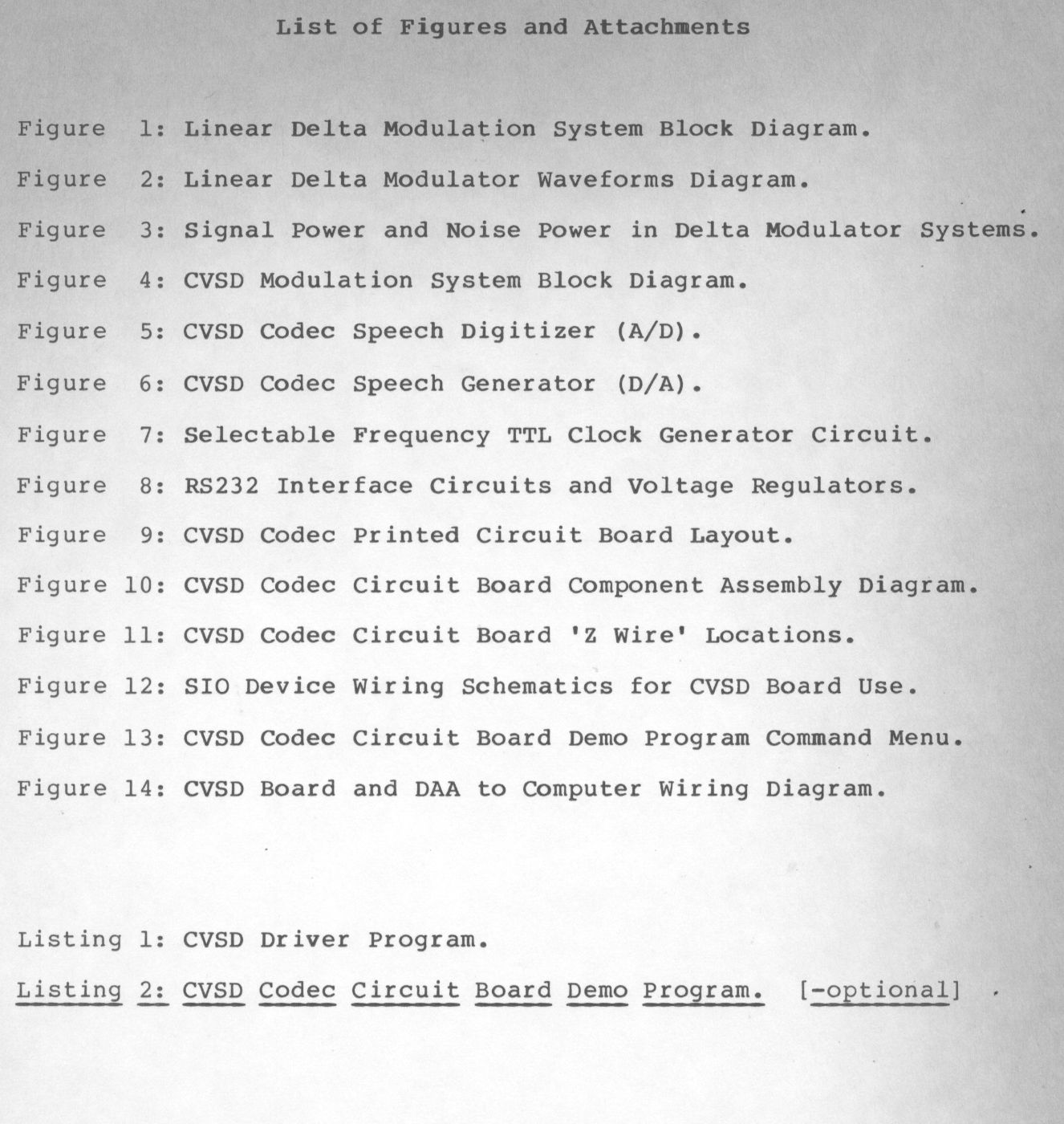
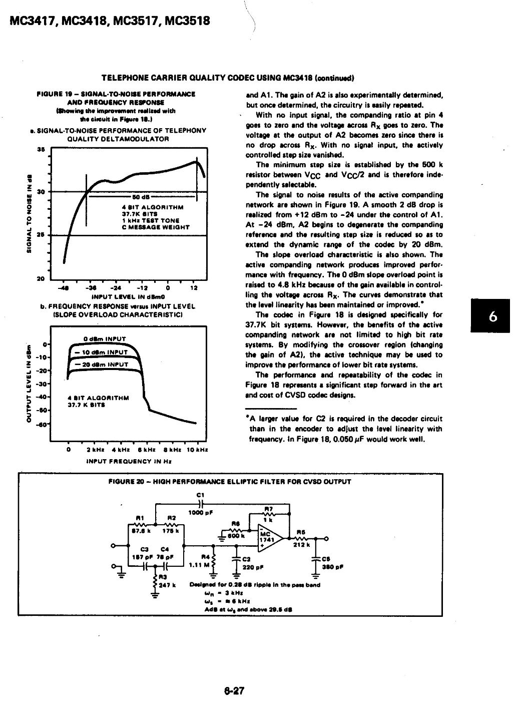
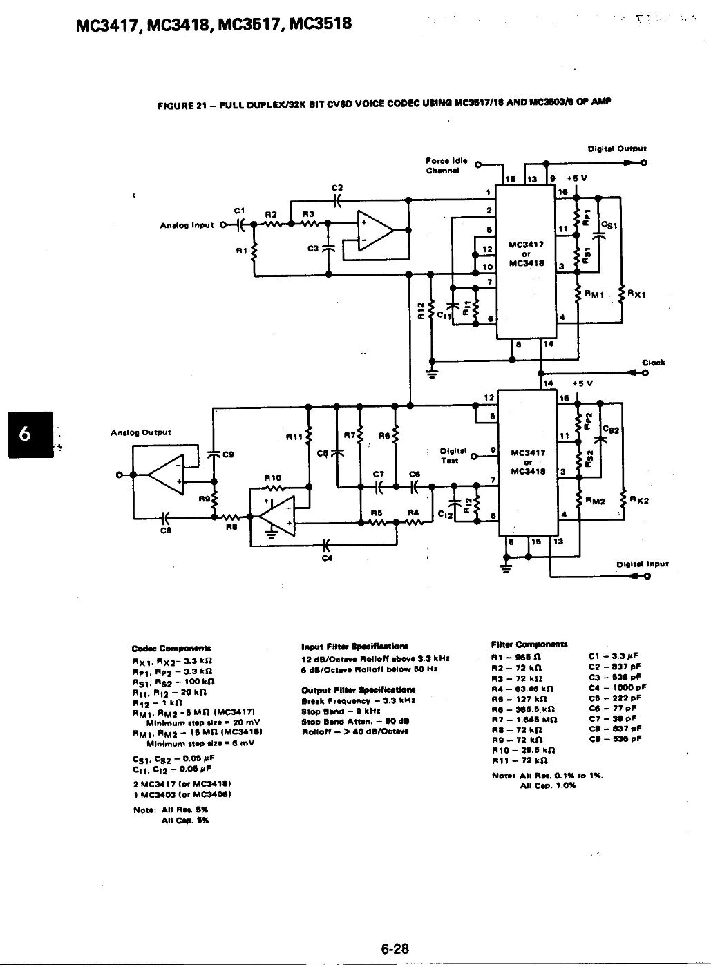
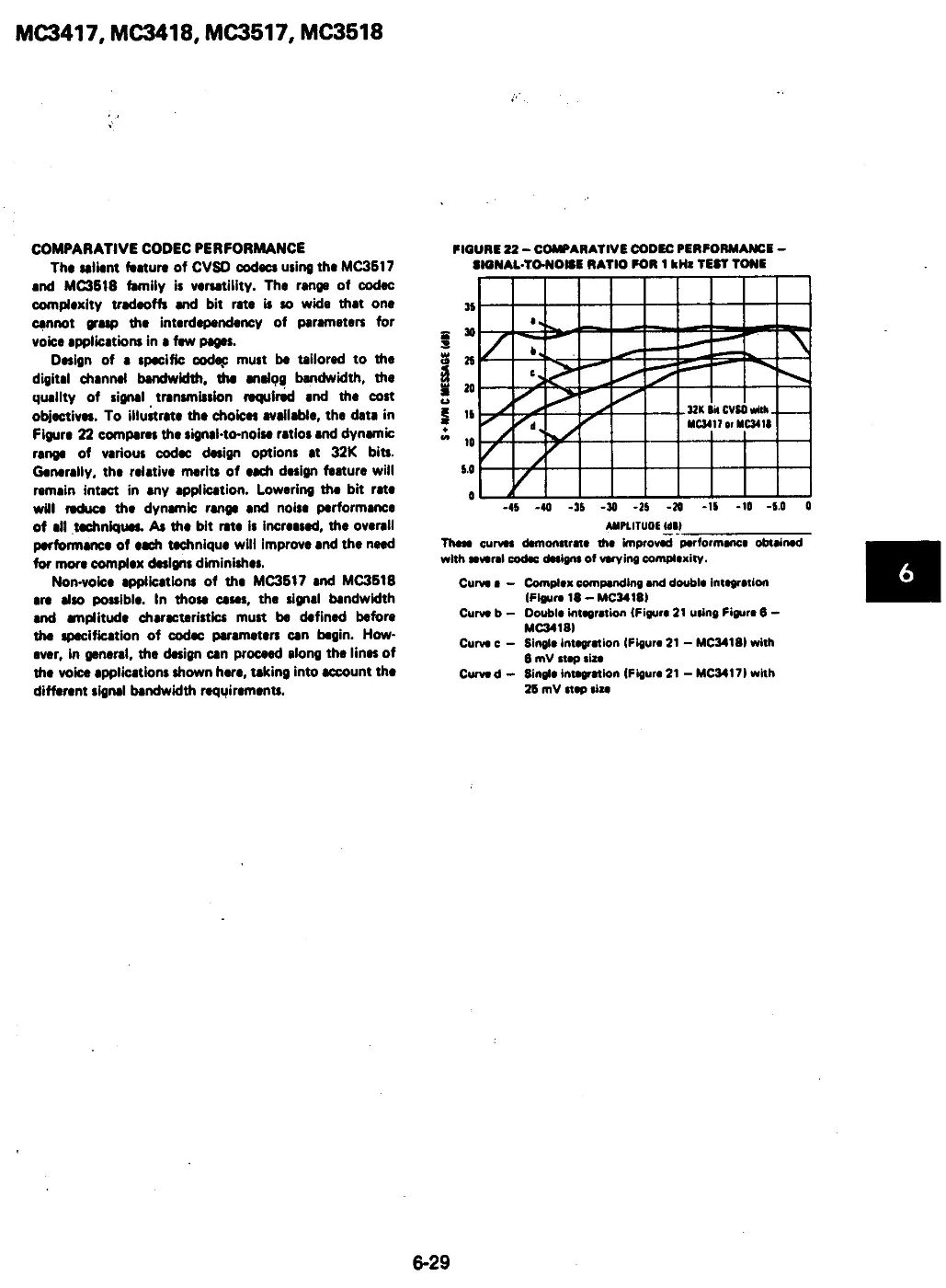
That concludes the article that was purchased by Radio Electronics magazine. Next below is a copy of the CVSD codec data sheet from Motorola. This document is very interesting and informative.
Conclusion
Hopefully you found some utility or interest in our screed presented above ☺ On a serious note Comments, Criticisms, and Suggestions are always appreciated. God bless all.

